scpmkj@gmail.com
Get A Free Quote

 share
share
With the rapid development of emerging applications such as 5G technology, autonomous driving, smart wear, and the Internet of Things, especially in industries such as communications, medical care, and industrial manufacturing, the market demand for chips as key components continues to surge. Data shows that the size of my country's chip market will reach 42.7 billion yuan in 2022, a year-on-year increase of 124%. It is expected that by 2024, the market size will further expand to 120.6 billion yuan.
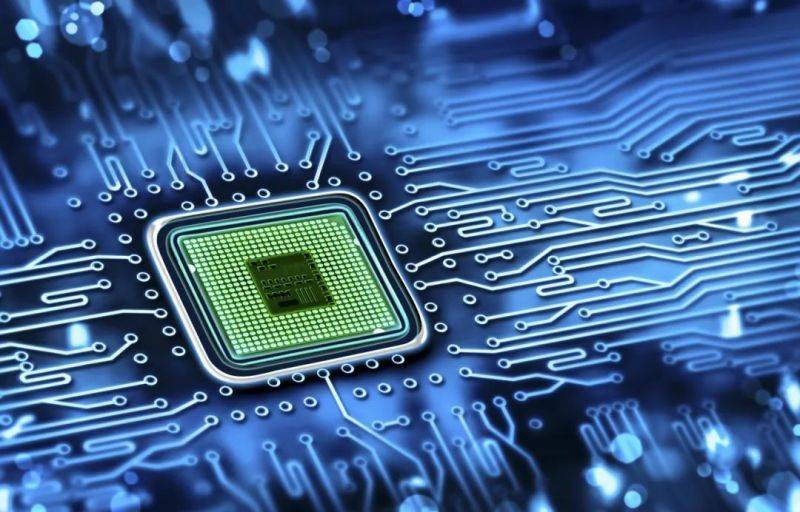
Laser chip Kaifeng Black Technology
Chip unsealing is also called chip uncapping or chip uncapping, which refers to performing local "surgical operations" on a fully encapsulated chip product, so that the internal structure of the chip can be exposed for detailed observation or other testing.
The purpose of opening the chip is to be able to clearly see the surface state of the chip, observe whether there are chipps and cracks in the chip scribe lane, and whether there are abnormalities on the surface, observe the chip logo information, measure the chip size and the bonding wire diameter, observe the bonding wire material, and observe the integrity of the passivation layer and other internal information of the chip. At the same time, we must maintain the integrity of the chip's functions and prepare for the next step of chip failure analysis experiments.
Laser chip unsealing technology uses high-energy laser to etch the plastic shell of chips or electronic components to achieve purposes such as optical inspection or electrical performance testing. This technology uses non-contact means to carry out high-precision and rapid peeling of the plastic coating layer, which can quickly remove local plastic coating materials without damaging the overall function of the chip substrate and circuit for testing or repair processing. Compared with traditional mechanical and chemical opening methods, laser chip opening technology is more efficient and yield, while avoiding the harm of strong acid environmental exposure.
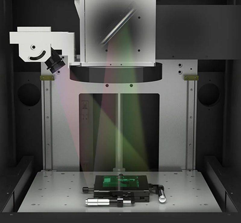
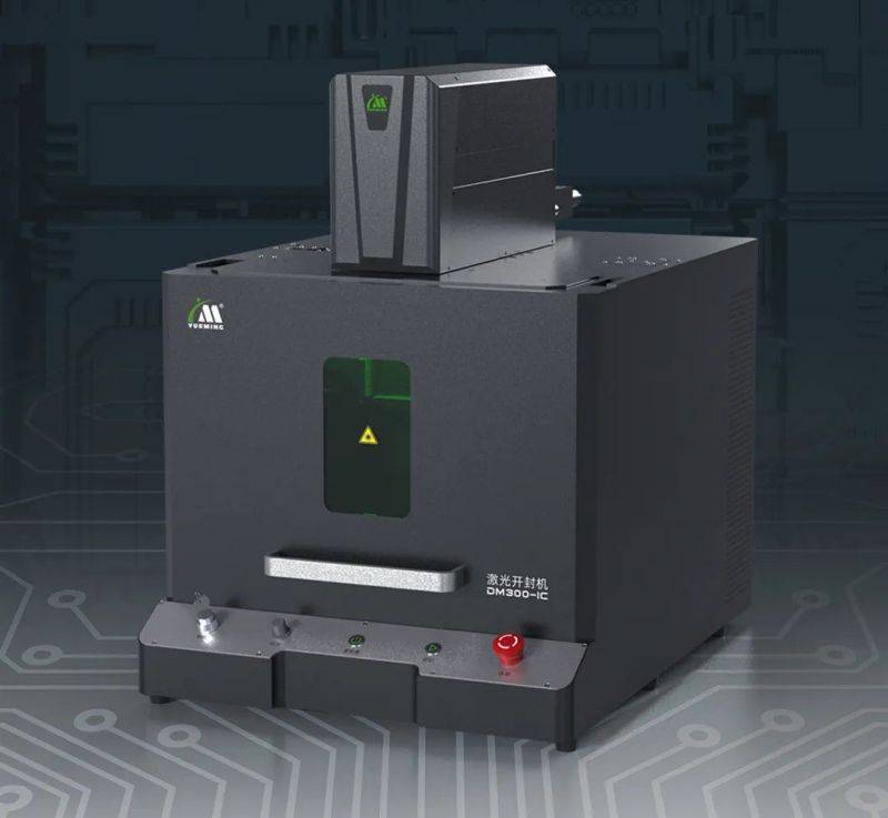
Yueming Laser Group Laser Chip Kaifeng System
Yueming Laser Group's laser chip opening system is professionally developed for the field of high-precision chip testing. It is convenient to operate, intelligent and efficient. With its ultra-high technological content and professional strength, it helps customers achieve high-quality and precise opening processing of chip products with the least amount of time and investment costs.
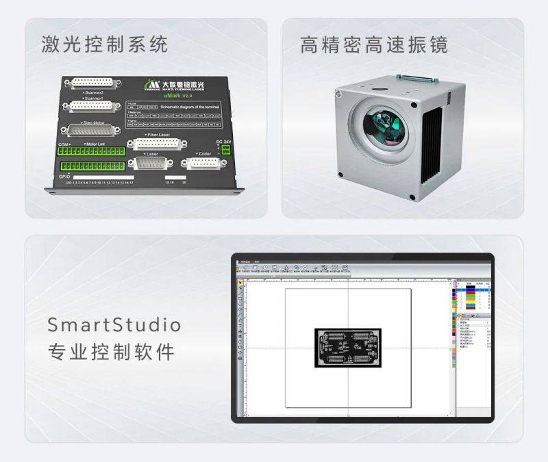
Dual CCD high-definition vision system
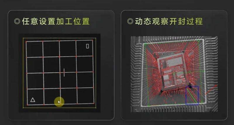
The dual CCD high-definition vision system is used to realize the full process of high-definition visual positioning and processing, high-definition color interface display, what you take is what you take, and real-time monitoring, recording and analysis of the processing process, effectively ensuring the accuracy and perfect effect of chip opening processing.
Independent research and development of three core modules
Yueming Laser Group's chip opening system is equipped with three core modules independently developed by Yueming Laser Group: laser control system, high-precision high-speed galvanometer, and SmartStudio professional control software. It has a high degree of automation, stable and lasting performance, scalability and compatibility., professional for opening high-precision chips.
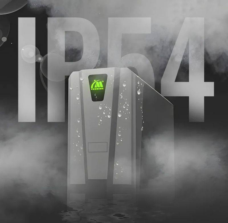
Highly integrated optical sealing system
Yueming Laser Group's chip opening system adopts a highly integrated optical sealing system with a double-layer sealing design. The protection standard reaches IP54 protection level. It is strong against dust, dirt, collision and water vapor, and is not afraid of harsh processing conditions and environment. Equipped with a multi-stage filter smoke purifier, the division of labor collects dust and removes odors, and the dust generated during work is purified and extracted in a timely manner to ensure the quality of chip opening and green production.
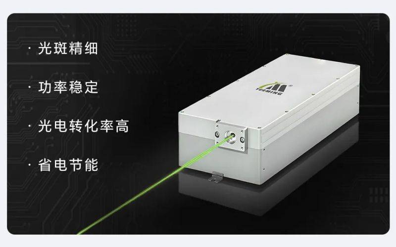
Professional laser light source does not damage the substrate
It adopts high-quality professional laser light source with stable power output, fine light spot, and precise control to ensure the integrity of the underlying materials and internal structure during the opening process. And the photoelectric conversion rate is high, which saves electricity and energy.
Yueming Laser Group's laser chip opening system adopts an integrated intensive design. The whole machine is small in size, occupies small space, and can be flexibly placed and used. Desktop-style connection method, simple and easy-to-understand interface, simple and convenient operation, intelligent and efficient. It is suitable for high-precision processing such as laser chip unsealing, component laser cutting, and component laser thinning in 3C electronics and automotive electronics industries. It is widely used in technology-based enterprises, laboratories of colleges and universities, scientific research units, testing institutions and other fields. It has successfully settled in many key universities, well-known laboratories and scientific research units, using high-precision and cutting-edge laser technology to "help" China's chip industry break through and promote the rapid development of China's chip industry.